|
||
|
|
|||||||||||||||||
|
Empowering High-Voltage AC Applications with Monolithic GaN | ||||||||||||||||||
|
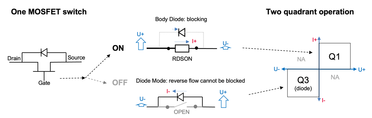
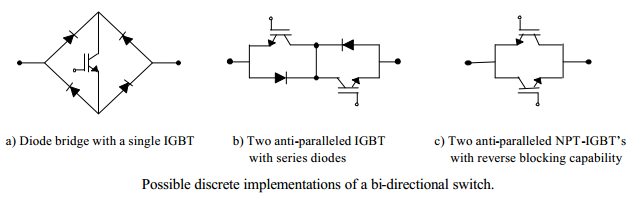
The challenge with most semiconductor switches is that they are inherently unidirectional, only controlling current flow in the first and third quadrants of the ac cycle, as shown in Fig. 1. There are several well-established BDS circuits, as seen in Fig. 2.
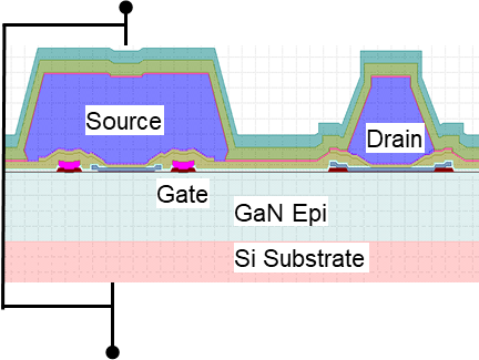
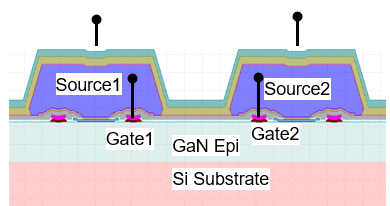
What do these have in common? They all integrate multiple devices (at least two and up to five) to create a BDS. These switches also suffer from on-state voltage offsets caused by the series diode and/or the IGBT, which cause conduction losses. And low-resistance diodes, which circuit designers prefer for these topologies to minimize those losses, are costly. Infineon's response to this challenge takes advantage of the work we have done developing gallium nitride high electron mobility transistors (GaN HEMTs). We use GaN because it is a wide-bandgap semiconductor, which can sustain higher voltages, switching frequencies, and operating temperatures than silicon (Si). Fig. 3 shows a cross-section of one of our GaN HEMTs.
Because it is difficult to make GaN crystals in commercial wafer sizes, we use silicon as a substrate. We then grow a thin layer of aluminium gallium nitride (AlGaN) on top of a thicker layer of GaN that has already been grown on top of that silicon substrate. The differing electrical properties of the AlGaN and GaN layers lead to the formation of a two-dimensional electron gas at the top of the GaN layer, which acts as the device's channel and provides the performance advantages of high electron mobility.
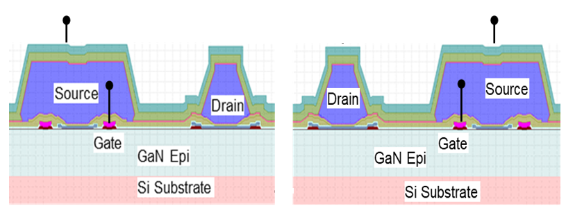
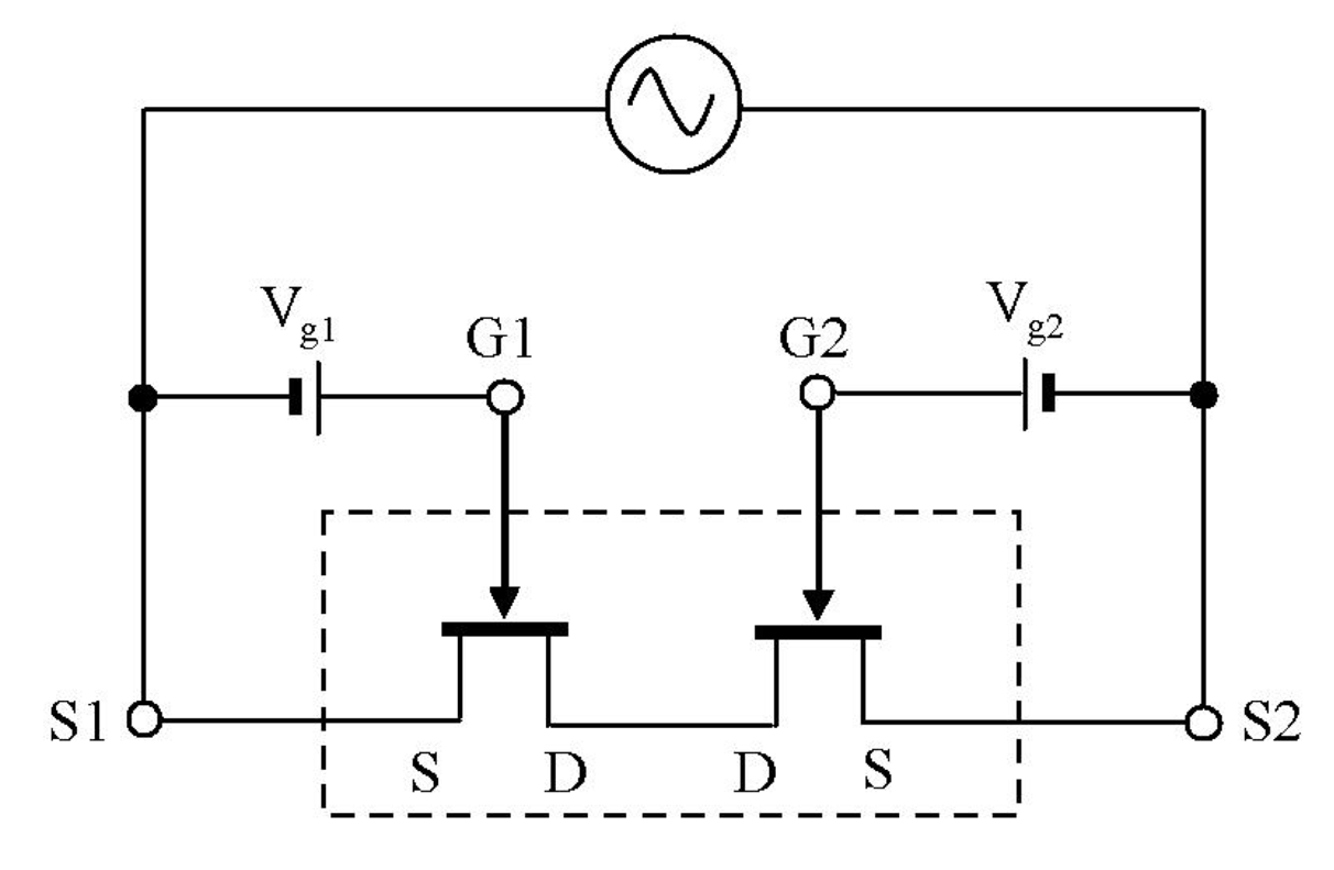
We could build a BDS by connecting two GAN HEMTs back-to-back, as in Fig. 4, but it would entail integrating two bare die or interconnecting two packaged parts, with the associated costs and reliability issues. Rather than do this, Infineon has integrated two GaN HEMTs into a monolithic BDS, illustrated in Fig. 5.
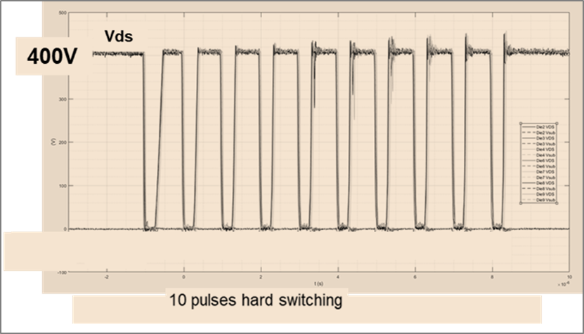
The gates of the two devices now share one channel, their drains are merged, and the device can control current in all four quadrants of the ac cycle using only those two gates. Fig. 6[1] shows the equivalent circuit of the monolithic device. The concept for this device originated in work done by Infineon's GaN partner Panasonic.[1] However, Infineon has carried the work forward, overcoming certain limitations in the original concept, and taken the lead in commercializing the monolithic GaN BDS. This device's architecture and implementation has several advantages. It doesn't accumulate and then have to dissipate a reverse recovery charge (QRR) during switching, which takes time and leads to heating losses in other device architectures. Minimizing the "deadtime" caused by this charge dissipation process also means that the device can be switched at higher frequencies than is possible with devices that have a high QRR. This in turn allows the resonant components of power conversion circuits, such as capacitors and inductors, to be smaller. The high electron mobility of the GaN device's channel means it is highly area efficient, achieving the same RDS(ON) as a silicon device in a quarter of the die area. The GaN BDS also offers lower—and more linear—input, output, and reverse-transfer capacitances than silicon equivalents making the device easier to drive in switching and commutation applications. The GaN BDS has other advantages. The product of its on-resistance and output capacitance (RDS(ON) x COSS) is about half that of an equivalent switching function built using back-to-back silicon superjunction MOSFETs. The product of its on-resistance and output charge (RDS(ON) x QOSS) is one tenth that of the silicon approach, and the product of its on-resistance and the energy dissipated by COSS (RDSON x EOSS) is 1.3 times less than in silicon. The benefits of the reduction of these factors compared to silicon devices is revealed in the practical switching characteristics of a GaN HEMT BDS. In a soft-switching boost converter design, switching at 500 kHz with a peak current of 1.8 A, the device delivered essentially clean output waveforms. The same is true in a double-pulse setup, hard switching 400 V at 1 MHz with a peak current of 6 A (Fig. 7).
The GaN HEMT BDS has several additional advantages over the silicon alternatives. Its monolithic format means designers don't have to specify and integrate up to five silicon devices to achieve the same BDS functionality, reducing packaging and assembly costs while also increasing reliability. Gate-drive characteristics are like those of the silicon alternative, although the GaN BDS device does need an additional supply to act as a separate reference voltage for its second source terminal. The area efficiency of GaN devices leads to smaller devices and therefore denser target implementations; we're beginning to see the effect of this in the latest generation of laptop chargers. The GaN BDS can also handle higher switching frequencies and faster transients than silicon, reducing the size of associated magnetic components, electromagnetic interference issues, and related mitigation costs, and enabling denser designs. We believe this technology will first be used to replace silicon circuitry in applications such as power factor correction, where it is a good match for the Vienna rectifier topology; in matrix and cyclo-converter circuits; and in disconnect switches. We also think it will be a good fit in new areas, such as single-stage conversion between dc and ac, ac and ac, and dc and dc, as well as in HV and LV current source inverters. Beyond this is uncharted territory. However, before we try to reach that territory, we need to speed up the adoption of GaN HEMT BDSs, find ways to manage any thermal issues that arise from packing such relatively high-power devices into such small packages, and explore ways of integrating GaN driver circuitry into the BDS itself to achieve further performance improvements from an all-GaN device. Infineon is currently sampling its GaN HEMT BDSs with plans to begin full production sometime in 2024 utilizing its next-generation CoolGaN technology platform. References:
Editor's Note: This article was first published in the July 2022 issue of How2Power Today |
||||||||||||||||||
| <<-Contents | <-Previous | Page 14 | Next-> | ||||||||||||||||||
|
If you or anyone in your company is interested in getting on the distribution list for future issues of PSMA UPDATE, please send e-mail to: power@psma.com. Be sure to include your name and
|
||||||||||||||||||