|
||
|
|
||||||||||
|
New JEDEC Guidelines Help Designers To Realistically Predict Stability Of SiC MOSFETs In Applications | |||||||||||
|
by Thomas Aichinger, Infineon Technologies, Villach, Austria
Those who have yet to evaluate SiC as a replacement for silicon MOSFETs can confidently compare the alternative and take advantage of the high thermal conductivity, energy efficiency and operating frequency, and low thermal expansion of these wide-bandgap devices. This article will provide background on the SiC market, discuss the JEDEC guidelines and testing performed by Infineon and conclude with details on newly implemented test procedures. The Growing Demand For SiC MOSFETs These SiC advantages are causing fast migration as customers adopt the technology quickly. The market growth rate was 22.8% from 2021 to 2022,[3] and the SiC market is expected to reach $2.1 billion U.S. by 2026 from $1.1 billion U.S. in 2022. Compared to silicon MOSFETs, SiC devices offer several advantages such as wide bandgap, high drift velocity, high breakdown voltage, large critical electrical field and high thermal conductivity. They are also capable of working at higher current densities and temperatures. Growing implementation of SiC devices is occurring in automotive applications due to the increasing demand for hybrid and electric vehicles. Also, the increasing need for efficient industrial operations is creating a strong demand for SiC in factories. New JEDEC Guidelines And SiC Based on engineers' observations that fully reversible and more permanent threshold-voltage variations occur with SiC MOSFETs, JEDEC developed "Guidelines for measuring the threshold voltage (VT) of SiC MOSFETs," JEP183A, and "Guideline for Evaluating Gate Switching Instability of Silicon Carbide Metal-Oxide-Semiconductor Devices for Power Electronic Conversion," JEP195. These guidelines combined with extensive investigations at Infineon provide deep insight into characterization and long-term parameter stability of SiC MOSFETs that has resulted in a greater understanding and new test methods.
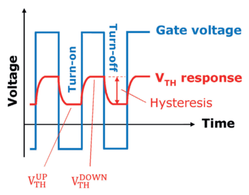
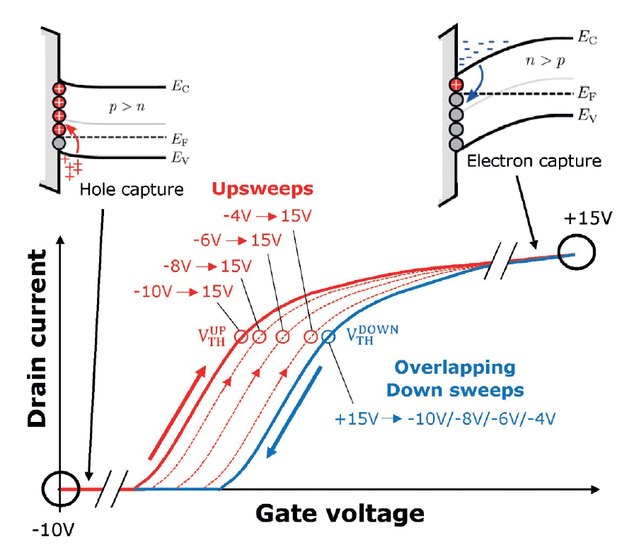
A stable and reproducible measurement of VTH is needed to define the datasheet values of "pristine" devices—these are parts that may have been tested but have not yet been used extensively or stressed. Also, it is mandatory for assessing VTH evolution in a stress experiment. Silicon MOSFETs do not require any particular precautions. Pristine silicon power transistors always show the same VTH. In contrast, SiC MOSFETs have a VTH that is not constant. Measurements of VTH show different values when the transistor turns on, coming from a negative gate voltage and when it turns off, coming from a positive gate voltage (see Fig. 1). This VTH hysteresis is the difference between the VTH during turn-on, the upsweep VTH (VTH-UP), and VTH during turnoff, the downsweep VTH (VTH-DOWN). Hysteresis is the largest when sweeping the gate between deep accumulation and deep inversion, for example, between -10 V and +15 V. Fig. 2 shows typical transfer characteristics of SiC MOSFETs for fast upsweeps and downsweeps of the gate voltage. Hysteresis reduces when the upsweep starts at voltages closer to 0 V and when sweeping is slower. Investigations suggest that these effects are due to short-term charging and discharging of preexisting traps located near or directly at the SiC/gate-oxide interface. The upsweep VTH is always lower because the interface is charged positively in the negative half period of the gate pulse due to holes captured from the valence band. Meanwhile, the downsweep VTH is always larger because the interface is charged neutrally or even negatively in the positive half period of the gate pulse due to electrons captured from the conduction band. Within the hysteresis envelope, there is a continuum of possible VTH values due to the large variety of capture and emission time constants for trapped charges in the virtually continuous defect band.
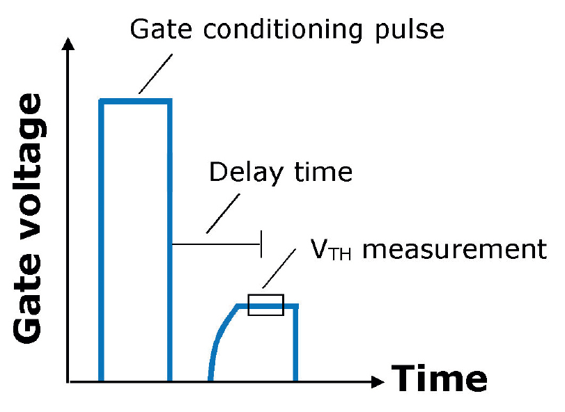
Improving Gate-Switching Stability One consequence of these findings is that the gate biasing history of the SiC MOSFET can impact VTH measurements for a very long time. For instance, when the device is either floating or biased at VGS = 0 V after the application of a positive or negative gate pulse, charges that are trapped near the mid-gap may be stored at the interface for hours, days or even longer. This stored charge keeps the device in a state of non-equilibrium. It results from the large thermal emission barriers associated with the wide bandgap of SiC. A comparable effect in silicon MOSFETs does not exist because they have a lower density of interface traps and a narrower bandgap. Based on these observations, obtaining reproducible VTH measurements with a SiC MOSFET begins by defining a gate-biasing history. One option is to apply a short positive gate pulse to the device using gate voltages between the recommended use voltage and the maximum allowed voltage in the datasheet (see Fig. 3). This technique is called gate conditioning. Once undertaken, VTH must be measured with a constant time delay. An easy way to accomplish fast, well-timed VTH spot measurements is to use a gated-diode measurement scheme. Here, the gate and drain terminals of the device are shorted, the source terminal grounded and a forced threshold current, for example 1 mA, is applied. Eventually, this gate-conditioning procedure creates a defined, reproducible charge state at the SiC/gate-oxide interface and enables a defined, reproducible VTH measurement.
Infineon research that is consistent with recent guidelines published by JEDEC showed that more-complex conditioning procedures, involving negative and positive gate-conditioning pulses, also allow for reproducible measurements of hysteresis.[4] With the process for measuring VTH in an accurate and reproducible manner defined, the next challenge was controlling and assessing VTH instabilities in SiC MOSFET operations. This was accomplished by developing a stress procedure for determining worst-case VTH drifts for different application profiles. Two more potentially application-relevant stressors were tested: the drain voltage and the load current. These studies revealed that neither led to altered VTH instabilities. The negative results allow a drastic simplification of the stress procedure without neglecting any important VTH stressors present in real applications. Another critical finding was the noticeable impact of the VTH increase on the RDS(ON) that differs among the voltage classes of the devices. The higher the voltage class, the more pronounced is the contribution of the thicker epitaxial layer's resistance. However, with M1H technology developed through the increased understanding of charge trapping phenomena and engineering of the SiC/gate-oxide interface, recently introduced 1,200-V CoolSiC MOSFETs excel in overall VTH stability. The end results of this extensive testing were that M1H technology was found to improve gate switching instability and enlarge the recommended gate-driving window. Applying the new test and stress guideline, CoolSiC MOSFET M1H devices demonstrate significant improvements in overall VTH stability. In particular, the application relevant drift caused by dynamic bipolar gate switching has been reduced significantly. As a consequence, the M1H technology offers the full window of gate voltages, even down to -10 V at the highest switching frequencies. The larger gate operation window provides maximum flexibility to customers and a high level of robustness against driver- and layout-related voltage peaks at the gate, with no restrictions towards higher switching frequencies. Finally, Infineon provides parameter drift evolution curves in app notes accompanying datasheets. These curves allow customers to directly extract the maximum drift that they can expect worst-case for a given technology during a specific application. Now, system designers can benefit from new test and stress procedures for SiC MOSFETs as well as predictability that can realistically determine their worst-case threshold voltage variations. Conclusion With an increased understanding of trapping dynamics at SiC's gate-oxide interface, new characterization and stress procedures have been developed specifically for SiC MOSFETs. These new methods provide standardized, reproducible measurements, as well as realistic assessments of time-dependent parameter variations in real applications. Now, engineers can predict how device characteristics will evolve during an application—even those applications that require 1,200-V SiC MOSFETs and very demanding requirements such as automotive. This paves the way for SiC MOSFETs to reach their next level of quality excellence and achieve projected market growth targets. Reference
About The Author
Since 2012 Thomas Aichinger has been part of the SiC MOSFET technology development team at Infineon Technologies, where he currently serves as lead principal engineer for SiC development. Thomas has been serving on the technical committee of IRPS and WiPDA and is currently serving as task group co-chair within the JEDEC sub-committee JC.70.2 focusing on SiC Power Electronic Conversion Semiconductor (PECS) standards. In addition, he has contributed to more than 80 scientific publications including journal articles, conference papers and book chapters. Prior to joining Infineon, Thomas was a postdoctoral researcher at Penn State University. He received his Ph.D. in electrical engineering from the Technical University of Vienna.
|
|||||||||||
| <<-Contents | <-Previous | Page 11 | Next-> | |||||||||||
|
If you or anyone in your company is interested in getting on the distribution list for future issues of PSMA UPDATE, please send e-mail to: power@psma.com. Be sure to include your name and
|
|||||||||||