
|
|
|
|
|
|||||||||
|
Mobile Apps Envision Merger of RF and Power Functions on a Single Chip | ||||||||||
|
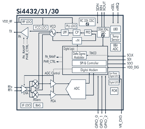
Integrating RF functions like power amplifiers and transceivers with power management on-chip has been a daunting task for designers. Nevertheless, this effort has been underway for several years now. Especially among RFIC makers who have been trying to optimize and miniaturize dc-dc converters so that they can be combined with RF functions on the same die. Hence, I will attempt to find answers to this challenge that has permitted a few to combine the two functionalities on a common semiconductor substrate, or bring them closer together in a single package, for use in the mobile space. Among the key semiconductor suppliers who have made significant progress on this front are Analog Devices, Silicon Laboratories, RF Micro Devices, Integrated Device Technology (IDT), and Nordic Semiconductor. IDT, for instance, is exploiting its experience in developing a variety of integrated PMICs for a myriad consumer devices and is currently looking beyond audio codecs and audio amplifiers. Consequently, it is now ready to push this level of power management integration to RF amplifiers and radio transceivers used in mobile handsets and cellular phones, including smartphones. For this integration, IDT is again tapping the benefits of using 0.18 micron BCD (Bipolar-CMOS-DMOS) process. This is the same process used to produce the previously discussed IDT P95020. As part of another ASIC chip solution, IDT designers are investigating a next-generation RF power amplifier that requires on-chip power tracking. That means, by monitoring the received signal level or strength, the system adjusts the power output of the RF amplifier. In other words, by dynamically applying the right amount of bias and voltage to the PA, it can adjust its output level so that the system can run more efficiently and effectively. The adjustable on-chip switching dc-dc buck converter used here achieves over 90 percent efficiency. And to ensure that efficiency remains high when the battery voltage goes low, a built-in switch disconnects the on-chip dc-dc converter and directly connects the battery to the amplifier. Since the drop from battery to PA is very small, the system efficiency remains high. By the way, to use a very small and low value inductor, the buck converter switches at 6 MHz. While keeping low-voltage and high-voltage circuits well isolated, the sophisticated BCD process also ensures that RF interference is minimal to keep on-chip power supplies clean for application-specific circuits like PAs and radio transceivers. In addition, with proper circuit design and layout, separating power and ground planes, the cross-talk and parasitics are minimized and interference is further curtailed, according to Siamak Bastami, IDT's director of Analog & Power Group. According to IDT, this forthcoming RF power amplifier with on-chip power tracking is expected to sample in the second quarter of this year. For high bandwidth and extended range wireless connectivity, Silicon Labs' has readied a wireless MCU that combines an ultra-low-power 25-MHz 8051 processor core with a high-performance sub-gigahertz RF transceiver called EZRadioPro. In this device, labeled Si1000, the RF transceiver and the microcontroller functions are on separate dies, but housed in a single 5-mm x 7-mm package. To keep current consumption low for battery power applications, the EZradioPro Transceiver (Si4432) incorporates on-chip six low dropout voltage regulators (LDOs), which also permits a wide operating supply voltage range from +1.8 to +3.6 V (Fig.1). In addition, the microcontroller die incorporates the switch-mode dc-dc converter that is used to power both the MCU and the radio functions of the Si1000. Meanwhile, LDOs on each die ensure on-chip voltage regulation. Both, the MCU and EZRadioPro dies are fabricated in a mainstream CMOS process.
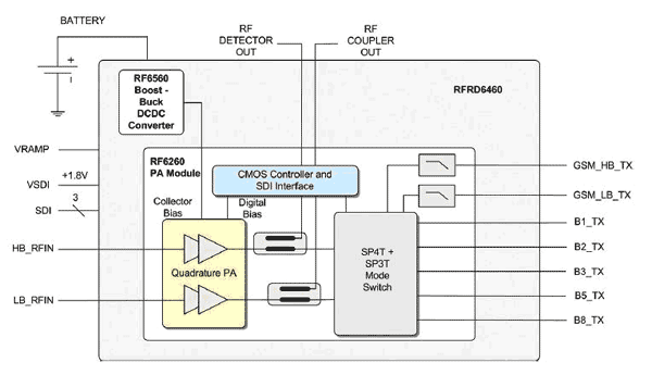
With smaller geometries, the RF transistors operate on lower voltages to keep current consumption low. And on-chip LDOs ensure that the supply voltages are within tolerance. The partitioning of functions on-chip is dictated by gate speed, RF performance and non-volatile memory, said Keith Odland, Silicon Labs' microcontroller product marketing manager. It is the process node that optimizes all these functions, added Odland. In the Si1000 solution, the microprocessor, along with its power management function, is on a separate die, Silicon Labs says it has the ability to create a monolithic solution if the application (or the customer) demands. "However, the two-chip solution gives us the flexibility, which turns out to be a better strategy for us," stated Odland. Another RF solutions provider addressing this level of integration is RF Micro Devices (RFMD). RFMD is also moving aggressively on this front as it recognizes that managing power within a mobile device is becoming extremely critical as more and more functions are added within a smaller footprint. Although the company has optimized a standalone buck dc-dc converter with more than 90% conversion efficiency to power CDMA/WCDMA power amplifiers (PAs), it has developed shielding, isolation and circuit techniques to bring such power supplies, including external passives, inside a multi-band, multimode PA multichip module. The result is the PowerSmart power platform (RFRD6460) with the ability to mitigate noise, interference and crosstalk in such an integrated RF solution.
While it is simpler to integrate power management and RF functions on a single chip in 2G or GSM handsets, the cost is a barrier. The 2G/GSM handset makers are not willing to pay high cost, says Ben Thomas, RFMD's director of marketing for 3G-4G cellular front ends. Yet another area where power management and RF functions are merging is Bluetooth. Ultra-low power specialist Nordic Semiconductor has released a new single chip Bluetooth v4.0 solution that integrates radio, baseband, microcontroller with fully embedded software stack, a stepdown dc-dc converter and a linear voltage regulator on the same CMOS chip. The on-chip dc-dc converter is specifically designed to lower peak current when operating from 3-V coin cell batteries. Labeled µBlue nRF8001, the Bluetooth v4.0 compliant wireless chip is housed in a 5-mm x 5-mm 32-pin QFN package. Expect to see continued developments along these lines in the future. In essence, as the process technologies advance and on-chip RF integration density increases, power management is becoming ever-more crucial. In this environment, the drive to integrate dc-dc converters, voltage regulators and other power sources becomes an important means of attaining time to market, performance and cost objectives. Provided by Ashok Bindra,
Ashok Bindra is a veteran writer and editor with more than 25 years of editorial experience covering RF/wireless technologies, semiconductors and power electronics. He has written, both for print and the web, for leading electronics trade publications in the U.S, including Electronics, EETimes, Electronic Design and RF Design. Presently, he has his own technical writing company called Technika through which he does writing projects for different trade publications and vendors. Prior to becoming an editor, Bindra worked in industry as an electronics engineer. He holds an M.S. degree from the Department of Electrical and Computer Engineering, Clarkson College of Technology (now Clarkson University) in Potsdam, NY, and an M.Sc (Physics) from the University of Bombay, India. He can be reached by email at bindra1[at]verizon.net. Editor's Note: This article was first published in the January 2011 issue of How2Power Today (www.how2power.com/newsletters). |
||||||||||
| <<-Contents | <-Previous | Page 8 | Next-> | ||||||||||
|
If you or anyone in your company is interested in getting on the distribution list for future issues of PSMA UPDATE, please send e-mail to: power@psma.com. Be sure to include your name and
|
||||||||||