
|
|
|
|
|
|||||||||||||||
|
New Technology Report Introduced at | ||||||||||||||||
|
Current Development in 3D Packaging With Focus on
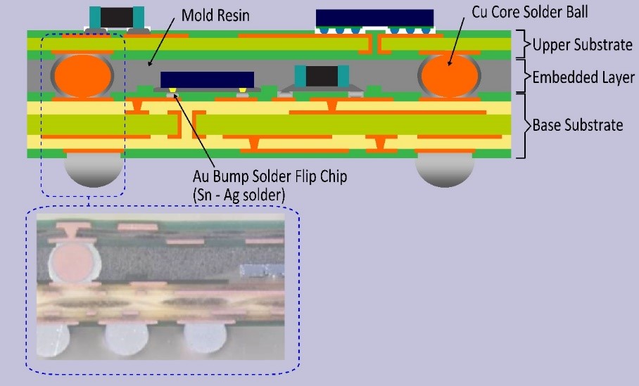
The PSMA Packaging Committee believes the 340 page report with extensive illustrations of the leading edge product technologies will provide valuable insights to executives and managers in their own analysis of how currently available materials and processes could be best used for the creation of advanced high efficiency, high power-density power electronic products. The report builds upon the findings of the Phase I report - 3D Power Packaging - issued by the Power Sources Manufacturers Association (PSMA) Packaging Committee in 2014. Background Let’s begin with a little background. The power electronics industry and the semiconductor industry are inseparably intertwined with one another, and both are facing unprecedented market challenges for efficiency, cost, construction and thermal issues which provide many opportunities for innovation. These industries are in the focal point of the “energy challenge” a multifaceted problem that involves mobile and cloud infrastructure systems, Internet-of-Things, renewable energy, smart grid, vehicle electrification, and across-the-board power efficiency enhancements in order to keep up with the industry's rapid growth in data consumption. These are the competiveness and sustainability challenges of the twenty-first century. The paradigm shift we have been experiencing in semiconductor packaging technology was brought about by advanced deep submicron semiconductor technology reaching a “cost barrier” that prevented further cost reduction by adding more functions to the semiconductor die. This barrier was circumvented through the development of wafer thinning that enabled through-silicon-via (TSV) technology, and the eventual introduction of 2.5D and 3D integration that facilitated heterogeneous (“More than Moore”) integration. It will allow the power requirements of the digital load to increase 2 to 5 times, within the same footprint, in a single generation. The power sources community must now find ways to package power sources that will meet this demand, but with no increase in footprint. In parallel, power semiconductor technology has been facing a “construction barrier” that prevents realization of the huge benefits new technology can offer in terms of increased power efficiency and higher power density. These new technologies which include gallium-nitrogen (GaN), silicon-carbon (SiC), and gallium-arsenic (GaAs) power semiconductor devices all require operation in an environment that is free of bond wires and minimizes parasitic interconnect elements. The best possible packaging technology to achieve this is embedding active and passive components in organic or inorganic substrates. Overview of the Report The report begins with a discussion of PCB embedding technology, which is fueled by the rapid evolution of low-power embedding and 3D packaging technologies, which are in high volume production. These technologies will in turn enable power electronic systems to deliver higher efficiency and higher power density.
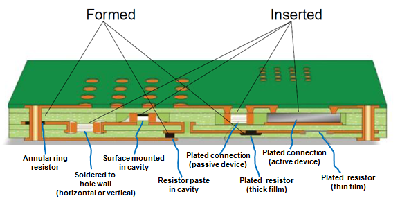
In addition to substrates the report dedicates entire chapters to each of the passive components (resistors, capacitor, and inductors) as well interposers and additive manufacturing.
The report also discusses high temperature die and component attach technologies that are evolving rapidly in the research labs; however, a single, low-cost, “one-size-fits-all applications” high-lead solder-substitution technology is currently unavailable and addresses the fact that high power-density component embedding and 3D packaging of power semiconductor devices also have to overcome a “thermal barrier.” Simply stated, it is more challenging to remove heat generated within the body of a 3D integrated system than from a planar, two-dimensional surface. This leads to a discussion of advanced thermal management technologies which are key enablers for 3D packaging as well as PCB embedding. The authors acknowledge and devote a chapter to the fact that high power-density component embedding and 3D packaging of power semiconductor devices also have to overcome a “thermal barrier.” Simply stated, it is more challenging to remove heat generated within the body of a 3D integrated system than from a planar, two-dimensional surface. This leads to a discussion of advanced thermal management technologies which are key enablers for 3D packaging as well as PCB embedding. In addition to their primary research, the team conducted a worldwide literature review and analysis of research and development (R&D) published by participating organizations in the USA, Asia-Pacific Region, and the EU, and identified several potentially high-impact technologies of interest to the power electronics and the semiconductor industries.. In terms of leadership positions, Germany and the EU appear to lead in the area of high-power PCB embedding and research into vertical interconnect/high-lead replacement technology, while Japan is leading in low power, high-density embedding, high performance, low CTE, high modulus (low warpage) substrates, and organic interposer technologies. Finally the report highlights some of the technology gaps as well as a recognition that this new technology requires updated or additional standards for manufacturing and testing. This report reviews the existing and pending new standards for PCB embedding which the IPC Association has taken the lead to author. However, much additional standard action is needed since the manufacturing supply chain is still evolving. Procedures need to evolve to establish compatibility of up-top metal-die design and PCB layout rules, testing, quality control, and for assigning ownership of failure. In summary, there has been substantial progress and excellent opportunities lie ahead for the power electronics and semiconductor industries and the entire manufacturing ecosystem to embrace PCB embedding and 3D packaging technologies for power electronic applications. The intersection of these technologies with the emerging wide-bandgap power semiconductor technology creates truly exciting possibilities at the same time the power electronics industry faces unprecedented challenges to help mitigate the fast growing demand for electricity and environmental problems our world faces. Embedded substrate packaging technologies can be, and will be deployed in hybrid and electric vehicles, alternative energy generation and distribution systems, smart grid, industrial, and military aerospace applications in the coming years and beyond. These technologies, combined with wide-bandgap semiconductor devices will literally re-vitalize the entire power electronic infrastructure block by block, module by module, for the twenty-first century. As a benefit of PSMA membership, the Current Development in 3D Packaging with Focus on Embedded Substrate Technologies report will be sent to all PSMA Regular and Associate member companies and Affiliate companies will be able to purchase the report at a reduced price. The report will also be offered to others in the industry at a price of $2990. You can view the report at the PSMA Exhibit booth at APEC 2015 and shortly the Table of Contents will be available on the PSMA website: www.psma.com. Submitted by the PSMA Packaging Committee.
|
||||||||||||||||
| <<-Contents | <-Previous | Page 8 | Next-> | ||||||||||||||||
|
If you or anyone in your company is interested in getting on the distribution list for future issues of PSMA UPDATE, please send e-mail to: power@psma.com. Be sure to include your name and
|
||||||||||||||||